How to Optimize HDI Circuit Boards for High-Speed Applications
HDI Circuit Boards for High-Speed Applications
In high-speed applications, signal transmission efficiency is a key factor in performance. To achieve better transmission, traces on PCBs should be as short as possible to minimize the amount of voltage drop along the length of the trace. This is also important to prevent interference with adjacent signals and to maintain proper power delivery. However, shorter traces can be challenging to design and can require more complex circuitry.
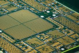
This is where HDI technology can help. HDI PCBs have a higher circuit density and offer greater miniaturization than standard multilayer PCBs. They can reduce the number of layers in a circuit board, without sacrificing quality or reliability. With advanced manufacturing techniques and materials, HDI PCBs can provide superior performance-price ratios for a variety of electronic devices.
An important consideration when designing an hdi circuit board is choosing the right components. This is because the selection of a component affects the routing width, location and types of vias, as well as the stack-up. Choosing the wrong components can significantly increase costs and lead to a delay in production, which can negatively impact a company’s bottom line.
How to Optimize HDI Circuit Boards for High-Speed Applications
Moreover, the choice of material used for an HDI circuit board is critical to its performance and manufacturability. These boards must be made from a material that is stable under heat, humidity and other environmental conditions. For example, copper is a common material for circuit boards because it has excellent electrical conductivity and is resistant to corrosion. However, FR4 is the preferred material for HDI boards due to its high temperature tolerance and good solderability.
In addition to reducing the size of a circuit board, HDI technology improves its signal integrity by allowing components to be placed closer together. This is done by using a combination of blind vias, buried vias and microvias. This can also reduce the overall height of the circuit board.
The use of stacked vias on HDI circuit boards also helps to improve the reliability of the device. Stacked vias can help to shield the circuit board from electromagnetic interference (EMI) and electrostatic discharge (ESD).
Another benefit of HDI technology is that it is more cost-efficient than traditional multilayer printed circuit boards. This is because HDI circuit boards use fewer raw materials than traditional PCBs. In addition, they can be produced in less time.
Compared to conventional multilayer PCBs, HDI circuit boards have a lower thickness of prepreg layers and fewer core layers. However, the main cost driver is putting the HDI circuit board through a series of lamination cycles. The process of putting the circuit board into the press, cooling it and waiting for it to gel is expensive. Hence, it is important to plan your orders in advance. This can help you to save money on the manufacturing costs and improve your business’s profit margin. Also, it is essential to choose a reliable supplier for your HDI circuit boards, such as MCL. They offer quick turnaround times and fast customer service, which can help you save a lot of money.