How Flexible Printed Circuit Boards Can Be Customized For Specific Applications
Flexible Printed Circuit Boards
Modern electronics manufacturers often face a conflicting set of demands when developing their products. These devices need to be lightweight and durable enough to meet consumer demands for portability and convenience, but they also must be engineered to accommodate a large number of complex connections in a limited space. And because manufacturing costs are often an important consideration, circuit integration must be performed as efficiently as possible. Fortunately, the introduction of flexible printed circuit boards (FPCs) has provided significant design freedom and lowered assembly costs.
As the name suggests, a flexible printed circuit board features conductive traces on a thin, flexible substrate. While they share many of the same characteristics as standard rigid PCBs, they differ from them in how they’re designed, manufactured, and functioning. This difference is largely due to the fact that these boards are designed to be able to bend.
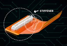
To be able to flex, these circuits must have a bending radius that’s sufficient to keep copper from being damaged by stresses in the surface. They also must have a layer structure that can reliably support dynamic bending. This means that they must have a minimum of three layers, with the ability to bend at different points on the board. Ideally, these boards should be made of materials that are both durable and low-cost.
How Flexible Printed Circuit Boards Can Be Customized For Specific Applications
These boards are typically constructed using a base material that’s flexible and durable, such as woven fiberglass impregnated with epoxy resin. Then they’re covered with a protective solder mask and silk screen, which provides the necessary conductors and connections. In terms of etching, the conductive copper paths are normally etched from metal foils, which can be made out of a wide variety of materials. However, copper is used for the majority of flex circuit applications because it’s both inexpensive and durable.
The flex circuits’ outer surface conductors are typically connected with plated through-holes or surface-mounted components. The circuits may also feature hold-down tabs, which are extensions of the copper pads that are anchored to the substrate. These can be utilized to hold the component in place during the assembly and rework process. To avoid stress concentration spots, flex circuits often utilize teardrop-shaped vias to connect the via to the copper trace.
The routing of traces is an essential part of designing a flexible circuit, and it can be challenging in some cases. To reduce the risk of errors, designers should always route traces away from regions that are prone to stress. They should also use annular rings, which are larger than the connecting traces to help prevent stress from building up around them. Finally, they should make sure that the traces are not running adjacent to each other near a bend area. This can increase stiffness in the bend areas and cause problems. Alternatively, they should stagger the traces. This will reduce stiffness and allow the traces to flex more easily.